
Microfocus X-Ray Generator Applications
Defect Detection
X-ray inspection is crucial for identifying defects in semiconductor wafers and packaged chips. X-ray imaging techniques, such as X-ray radiography and X-ray tomography, can reveal internal defects such as voids, cracks, delaminations, and wire bond integrity issues without damaging the device. This helps ensure the reliability and functionality of the final semiconductor products.
Quality Control
X-ray metrology techniques are employed for quality control purposes during various stages of semiconductor fabrication.
Wafer Inspection
X-ray wafer inspection systems are used to detect defects and anomalies in semiconductor wafers before they are processed further. These systems use X-ray beams to scan the surface and subsurface of the wafers, identifying defects such as particles, scratches, and pattern deviations that could affect device yield and performance.
Package Inspection
X-ray inspection is also performed on packaged semiconductor devices to ensure the integrity of the encapsulation and the solder joints. This non-destructive testing technique helps detect issues such as voids in solder balls, cracks in the package, and wire bond defects, which could lead to reliability issues in the field.
Failure Analysis
X-ray analysis plays a crucial role in failure analysis investigations of semiconductor devices that have experienced performance or reliability issues. By examining the internal structure of failed devices using X-ray microscopy and X-ray spectroscopy, engineers can pinpoint the root causes of failures, such as manufacturing defects, material degradation, or electrical overstress.
Other Microfocus Xray Inspection Applications
X-Ray Generators for the Semiconductors Industry
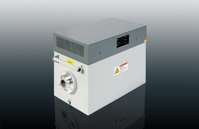
UC Series X-ray Generators
Gulmay’s Microfocus generator line up has grown to include generators ranging from 65kV up to 320kV. Read More
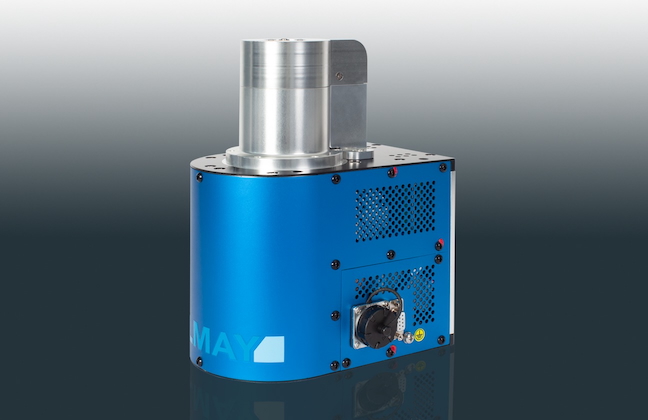
GMF Series Integrated Sources
GMF series microfocus X-ray sources offer outstanding performance and reliability in a compact package.Read More